Intel announces new roadmap at IFS Direct Connect 2024: New 14A node, Clearwater Forest taped-in, five nodes in four years remains on track

IFS now has a full roster of technologies and partners for its foundry business.

Intel unveiled a new roadmap that includes a new 14A node, the industry’s first to use High-NA EUV, here at its Intel Foundry Services (IFS) Direct Connect 2024 event. IFS also added new extensions to its existing lineup of process nodes and announced that it is now producing wafers of its Clearwater Forest processors on its 18A node. That’s yet another proof point that Intel’s audacious goal of delivering five nodes in four years (5N4Y) is on track for completion by the end of the year, thus giving Intel confidence that it will take back the process node leadership crown from TSMC with its 18A node in 2025. Microsoft also announced that it is building chips on Intel's 18A process node. 


As part of the coming out party, Intel has also renamed IFS to Intel Foundry. Intel Foundry has a goal of being the second-largest foundry in the world by 2030, and IFS Direct Connect 2024 is the company’s coming out party as a ‘systems foundry,’ an Intel-defined term that quantifies its experience with system-level design and includes all its technology development, manufacturing, supply chain, and the Intel Foundry Services under one umbrella. This includes not only producing processors of varying types, but also providing customers with packaging and connectivity fabric solutions - and even helping with cooling solutions. Intel Foundry caters to both external customers and internal customers from within Intel, with the goal of serving both equally (an important distinction) with a resilient and sustainable supply chain.


Now, on to the roadmaps (we also have an Intel vs TSMC and Samsung roadmap further below).

Five nodes in four years remains on track

We’ll get to the new roadmap next, but as you can see above, Intel CEO Pat Gelsinger’s original 2021 plan for five nodes in four years remains on track. The Intel 7 and Intel 4 nodes are now in market, and Intel 3 is ready for high volume manufacturing (HVM). Intel’s 20A (2nm) and 18A (1.8nm) are also on track for arrival as the first chips in the industry with both its PowerVia backside power delivery, which provides optimized power routing to improve performance and transistor density, and Intel’s first node with RibbonFET gate-all-around (GAA) transistors, which also provides better transistor density along with faster transistor switching, but in a smaller area. Intel’s 18A is now ready for its customers to design with the 0.9 PDK from Intel’s EDA (design software) and IP partners now, with the full 1.0 PDK arriving in the April/May timeframe.


Intel has now taped out Clearwater Forest, meaning that the chips’ final design is ready for production. Clearwater Forest is the company’s first high-volume 18A chip. As revealed in the above slide, Clearwater Forest is comprised of CPU tiles fabbed on the 18A node which are then bonded together with an Intel 3 base die using 3D Foveros packaging technology. The base die also includes cache. 

The Clearwater Forest design ropes in many of the architectural concepts we’ve seen with the Granite Rapids and 288-Core and 144-core Sierra Forest processors, but the new addition of 3D Foveros packaging is key. This tactic of bonding logic dies with a base die will also be critical in chip designs that use HBM4, which we’re told will require an active base die to ensure optimal signal integrity. As such, this tech will be incredibly important for the next wave of memory bandwidth-hungry AI chips.

Clearwater Forest is the first high-volume chip to use the Universal Chiplet Interconnect Express (UCIe), a new industry interface for connecting chips together. UCIe is a pivotal advance here that shouldn’t be overlooked: the interface is supported by Intel, AMD, Arm, Nvidia, TSMC, Samsung, and 120 others, to standardize the die-to-die interconnects between chiplets with an open-source design, thus reducing costs and fostering a broader ecosystem of validated mix-and-match chiplets from multiple chipmakers. Intel’s all-in approach with UCIe for Clearwater Forest signals not only that this tech is moving apace, but also that Intel is leading the industry charge.

BEYOND 5N4Y – THE ARRIVAL OF INTEL 14A AND CUSTOMIZED NODE EXTENSIONS

http://zeontechhk.com/wp-content/uploads/2024/03/8D57mmih2n4Dxq5QtUoDjT.jpg

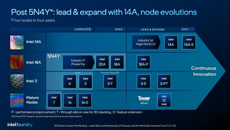
The Post-5N4Y chart shows us what’s next – the Intel 14A process. This will be the first process node in the industry that will use a High-NA EUV lithography tool from ASML. This new chipmaking tool will allow chipmakers to print smaller features than ever before, which Intel says will enable higher performance. In fact, Intel is the first company in the industry to receive a cutting-edge High-NA tool, while TSMC is said to have delayed using the tool until 2030 due to cost concerns. Intel Foundry head Stu Pann tells us that the tool is cost-effective for Intel’s purposes, mirroring ASML’s comments on the matter.

Intel isn’t sharing performance or density targets for 14A yet, saying that it doesn’t want to give its competitors a target yet. However, we do know that it will come with next-gen PowerVia backside power delivery (likely Source-on-Contact) and RibbonFET GAA transistors. Intel has two flavors of 14A on its roadmap – the standard 14A, and then a follow-on extension called 14A-E. The E stands for a feature extension, which is part of Intel’s new approach of delivering different customizations of existing process nodes to extend their lifecycle, just like TSMC and Samsung (more on that below).

Intel isn’t committing to a date for the first 14A revision, though we do know that it arrives after 2024. The second 14A-E revision will go to risk production, meaning the first test chips will be made on A0 silicon, in the 2027 timeframe. Given Intel’s return to a Tick-Tock-like cadence and the timing of 14A-E, we think it’s safe to assume that 14A will arrive in 2026. As with Intel’s other leading-edge nodes, 14A will be developed in Oregon and then mass produced at other facilities (these remain unspecified for now).

Intel will also extend its Intel 7, Intel 3, and Intel 16 node with new ‘line extensions.’ Intel plans to deliver a new node every two years, and then sprinkle in line extensions every other year, much like its old Tick-Tock model. These line extensions are denoted by new suffixes.

The P suffix indicates a new revision of the node with performance improvements, the T suffix is for TSV-equipped nodes that can used with hybrid bonding/3D Foveros, and E suffixes indicate specialized new features, like tuned operating/voltage ranges. Intel will also have PT revisions that indicate both performance and special features, and we expect that other combined revisions will emerge over time. This technique will allow Intel Foundry to extract further use from existing nodes to serve specific customer use cases.

Intel will also have its new Intel 12 node arrive in the coming years, which comes as the fruits of its new manufacturing collaboration with UMC. Intel Foundry is also producing mature-node 65nm chips for Tower Semiconductor. Both of these collaborations are key to building further scale for Intel’s IFS operations while allowing the company to extract more value for its already depreciated tooling and facilities.

INTEL VS TSMC VS SAMSUNG PROCESS NODE ROADMAP

The above roadmap is based on publicly available information, but be aware that it doesn’t include several of the most important PPAC (Power, Performance, Area and Cost) metrics. However, it does give us a solid timeline of future process nodes from Intel, TSMC, and Samsung. You can also see that TSMC and Samsung also use multiple line extensions of the same node, just like Intel now does as well (for instance, TSMC’s N3B, N3E, and N3P)

Samsung was the first to bring gate-all-around (GAA) transistors to market back in 2022, but its implementation hasn’t been very performant and suffered from poor yields, leading to further market share losses to TSMC. This also highlights that having a technology doesn’t always assure success – the implementation matters.

Intel’s 20A and 18A come with both GAA (PowerVia) and the backside power delivery network (BSPDN), Intel will have backside power delivery two and a half years before TSMC and will also beat TSMC to market with GAA by a year and a half. As we’ve seen with Samsung, which remains the dark horse of the leading-edge foundry industry, having these technologies doesn’t always ensure a win. However, if the critical PPAC metrics align correctly, Intel’s early adoption of these technologies will give it a significant advantage over TSMC.

Finally, as we can see, 14A will mark Intel Foundry as being the first foundry to use the most advanced High-NA EUV lithography machines, with TSMC reportedly waiting until 2030 to adopt the new tools. High-NA will certainly not be an inexpensive path, and an industry report indicates it isn’t as cost effective as using Low-NA EUV with dual patterning. Intel is confident that the cost metrics align within its expectations, but naturally, says it would adjust strategy if needed.

EDA CHIP DESIGN SOFTWARE AND A FULL SUITE OF PACKAGING OPTIONS

http://zeontechhk.com/wp-content/uploads/2024/03/izuGKKh58T8Sn72hRSEytT.jpg

Intel secured four large 18A customer commitments in 2023, and one includes a large prepay for foundry capacity, implying that it is for a very significant quantity of processors. Microsoft has also announced that it will fab a chip on Intel's 18A process, a major buy-in from one of the industry's largest players.

The company has also won design wins across its Intel 16 and Intel 3 nodes and has won significant deals for its Intel Foundry ASAT packaging services, including lucrative advanced packaging contracts with EMIB, Foveros, and Foveros Direct.

The Intel Foundry Services Accelerator program helps chip designers and companies easily adopt Intel’s manufacturing technologies. This program includes 34 partners spread across four alliances: IP, EDA, design services, and USMAG (US Military, Aerospace and Government). This wide range of partners include EDA industry heavyweights like Ansys, Cadence, Synopsys, Siemens and Keysight, along with a wide range of IP partners that include Arm, RISC-V, SiFive, Rambus, and others.

THOUGHTS

As mentioned in the preceding section, Intel Foundry has significant customer wins with all of its foundry offerings. Microsoft has also announced that it will fab a chip on Intel's 18A process, a major buy-in from one of the industry's largest players. 

Intel also has extensive experience in chip packaging and test along with an impressive portfolio of leading-edge packaging technologies for its customers, as we recently saw firsthand when we toured the company’s packaging facilities in Penang, Malaysia, which has led to a sudden increase in packaging contracts for AI chips.

Intel CEO Pat Gelsinger recently noted that five years ago packaging comprised 15% of the total cost of a leading-edge processor, but that has now jumped to 35 to 40% of the total cost. As such, Intel’s advances in its packaging business should not be ignored, particularly given that it also helps the company establish new ties with customers that might elect to also use the company’s chip-making services.

Intel Foundry is also partnering with Arm to bring Neoverse chips to its foundries, a critical step to gaining production volume, and its work with the Department of Defense on the RAMP-C program that has already yielded a billion-dollar award, along with possible future contracts from the US defense industrial base. That’s not to mention its existing partnerships with RISC-V and SiFive, among others.

Intel’s extensive portfolio of EDA and IP partners will now provide industry-standard design tools for Intel Foundry customers, thus offering an easy on-ramp for companies to quickly adopt the Intel process nodes. Paired with a bevy of process nodes and a wide range of packaging services coupled with systems-level design experience, IFS is clearly poised to compete fiercely with TSMC and Samsung for third-party foundry customers in the coming years.

You can read more about those efforts in our interview with Stu Pann, the SVP and GM of Intel Foundry Services, who is tasked with making Intel Foundry the world’s second-largest foundry by 2030.


© 2023 Zeon Technology